
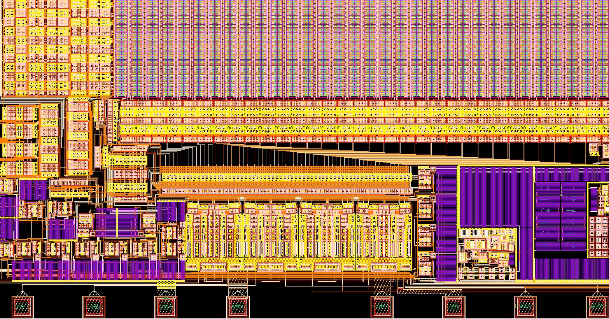
DESIGNS
| SOFTWARE | MODULES |
|---|---|
| Cadence | Analog, Digital, RF and mixed signal |
| Coventor | MEMS+, CoventorWare, SEMulator 3D |
| Keysight Technologies | IC-CAP |
Physics Simulation
Study the physical properties of devices and materials for MEMS or ASIC applications, including the material properties and underlying physics. Study and simulate the mechanical, electrical and structural properties of devices, as well as propose viable engineering solutions.
Mixed Signal Circuit design
Team of experienced individuals provides design solutions for Analog and Digital CMOS designs such as ADCs, DACs, amplifiers, and memory devices.
MEMS
Mechanical and layout design for MEMS devices through Coventor software and translated to fab-ready layout that can be adapted to SEMC facilities or externally.
Consultation
Provide insight and recommendations for material and physics for the selected designs by utilizing the expertise at SEMC to provide clients with complete solutions spanning the design, schematics, layout, and simulation, for custom designs or any of the available 500+ IPs owned by SEMC. The design department is equipped with state-of-the-art software options and solutions that allow for complete solutions from physics and schematics to layout, to ensure seamless integration with the facility at SEMC.
PRODUCTION

| PROCESS | TECHNOLOGY |
|---|---|
| Dry Etching | ICP RIE etching, polymer removal, and deep Si etch |
| Thermal Processing | Thermal oxidation, annealing, LPCVD |
| Wet Etching | RCA cleaning, polymers removal, megasonic cleaning, metal and oxide etching |
| Photolithography | Automatic spray coater, laser writer, mask aligner, and electron beam lithography |
| Deposition | PECVD, sputtering, ALD, and evaporation |
| In-line Measurement | Ellipsometry, sheet resistance, TCR, thin film stress, laser profiler, needle profilometer |
| Ion Implantation | Medium voltage implanter with several dopant species (P, As, B) |
CMOS/MEMS R&D
SEMC production team has established great capabilities in research and development, especially in the technologies of MEMS and CMOS. The facility is equipped with state-of-the-art tools and is run by top notch personnel and process engineers.
Process Consultation
The Production team at SEMC has immense experience in several cutting-edge technologies including MEMS and CMOS and can offer their expertise in developing and integrating processes and recipes to reach the specified objectives. The services can include product performance metrics against the process flow and tool performance.
Infrastructure Assessment
Facility level and Equipment level consultations, as well as planning, and assessment can be provided by an experienced team from SEMC capable of ensuring excellent adherence to cleanroom protocols and procedures.
Thin Film Deposition
SEMC excels in the deposition of many thin films with control over its properties according to latest literature yet also allow for pristine quality and condition. There are several thin film deposition techniques and thin films at SEMC, as follows:
| TECHNOLOGY | THIN FILM |
|---|---|
| LPCVD | Si3N4, pSi, aSi, TEOS |
| PECVD | SiNx, SiO2, TEOS |
| Sputtering | Al, Ti, Nb, Mo, TiN, V, Cr |
| ALD | HfOx, Al2O3, Ta |
| Oxidation | Furnace Dry and Wet SiO2 |
Cleanroom Monitoring and Quality inspection
SEMC team has the experience and capability to provide monitoring recommendations and quality inspection to ensure that the high standards followed at SEMC can be transferred to other foundries and laboratories. This service covers crucial parameters such as temperature, humidity, and particle count as well as gas monitoring and purity verification.
Process Training
SEMC production team has established great capabilities in research and development, especially in the technologies of MEMS and CMOS. The facility is equipped with state-of-the- art tools and is run by top notch personnel and process engineers. Several training programs can be provided by the production team, aimed at specific tools and essential processes.
Non-destructive Inline Analysis techniques
SEMC offers advanced tools and capabilities for inline analysis, measurement, and characterization. This service allows for the investigation of failure causes, through a plethora of in-line measurement and analysis techniques operated by professional personnel.
NANO-ANALYSIS AND REVERSE ENGINEERING
IC Imaging Techniques
SEMC owns many techniques for imaging and analyzing on nano-meter scale, including optical microscopes, Scanning Electron Microscope (SEM), Energy-Dispersive X-ray (EDX), Focused Ion Beam (FIB) and Plasma Focused Ion Beam (PFIB).
IC Failure Analysis Technique
The IC failure analysis process is a systematic investigation to identify the root cause of failures. It begins with collecting failure information and performing non-destructive tests. Next, fault isolation techniques like Liquid Crystal Hot Spot Detection (LCHSD) are used to pinpoint the defect location. The final stage is destructive analysis to physically identify and analyze the defect.
IC Cross-Section Technique
The IC cross-section nano-analysis techniques are essential techniques for identifying defects, verifying structural integrity, and conducting failure analysis, they involve a multi-step process of sample preparation followed by high- resolution imaging and elemental analysis.
IC De-Processing Techniques
This method is used to selectively remove layers to enable nanoscale analysis. It is are essential for failure analysis and include both "top-down" de-processing, which removes layers from the surface, and "backside" de-processing, which removes material from the back of the chip. They often use a combination of physical and chemical processes like Focused Ion Beam (FIB) milling and Reactive Ion Etching (RIE).
IC Delineation Technique
It is one of the most sophisticated nano-analysis techniques, used to separate and identify ionic species, which is then used in conjunction with other analytical methods to characterize nanoparticles.
IC Reverse Engineering (RE) Technique
The IC reverse engineering process involves extracting and analyzing a microchip's internal circuitry to understand its design, architecture, function, interconnections and firmware, by observing and analyzing the chip and the package. The RE main goals include interoperability, security research, failure analysis and academic research.
WAFER LEVEL CHARACTERIZATION
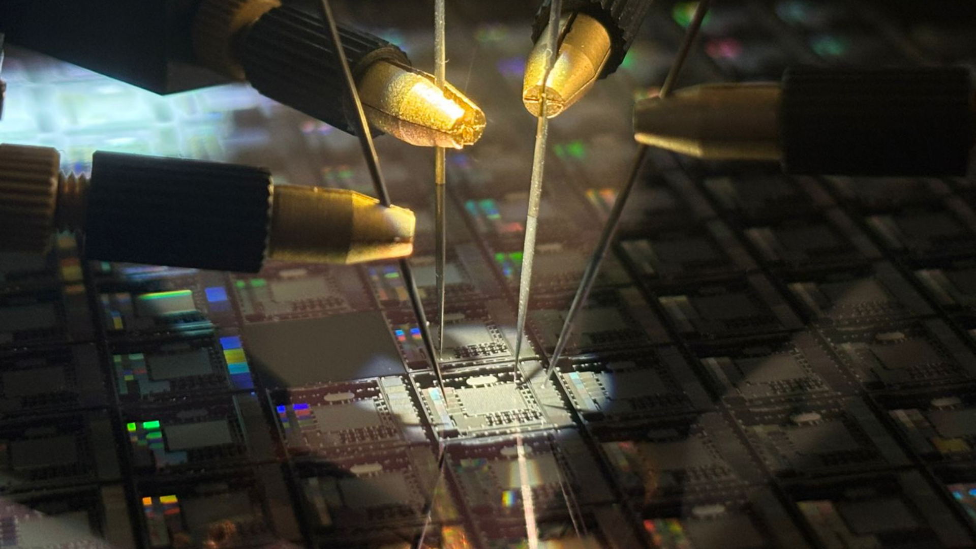
Transistor Characterization
Measuring current s and volta ge s (I-V characteristics ) . Extracting transistor characteristics such as gain, saturation current, and threshold voltage. Analyzing transistor behavior under various operating conditions.
Diode Electrolysis
Measure current-voltage (I-V) curves for various types of diodes (standard, Zener, Schottky). Determine breakdown voltage, forward bias voltage, and reverse current.
Semiconductor Material Quality Verification
Measure the sample resistance (resistivity). Analyze impurities and their effect on electrical properties.
Component Reliability and Stability Testing
Tests under constant temperature or voltage conditions for extended periods. Evaluate component performance over time.
MEMS In-plane and Out-of-plane Characterization
It is one of the most advanced nano-analysis techniques used in semiconductor labs, where the Polytec MSA (Micro System Analyzer) - an optical measurement system- uses Laser Doppler Vibrometry (LDV) and stroboscopic video microscopy to characterize MEMS devices without contact. It measures 3D vibrations and displacements of microstructures like beams, membranes, resonators, accelerometers, and microphones.
SYSTEM LEVEL CHARACTERIZATION
Angular rate velocity Setup
This is a multi-degree of freedom test stand that allows testing of a wide variety of inertial navigation packages, sensors, and other components requiring precision motion as a test input.
Temperature & Humidity Chamber Test
Temperature & Humidity Chamber test allows the desired sensors and systems under a verity set of temperatures with humidity monitor readings. Limitation: Temperature Ranges from - 70 °C to +180 °C
Vibration Test
The vibration Test is an electrodynamic vibration test system used to simulate real-world mechanical stresses such as vibration and shock on components, assemblies, and materials.
Shock Exciter (Drop) Test
The Shock Exciter (Drop) Test Setup is a pneumatically driven shock exciter engineered for precision shock testing and secondary calibration of shock transducers, accelerometers, and complete measuring chains.
System Noise Measurement
The noise measurement setup is a test station that is used to measure and validate the noise in a bolometer structure or any packaged sensor. The noise is typically measured over a frequency range. Frequency range of the system from 2-200 KHz.
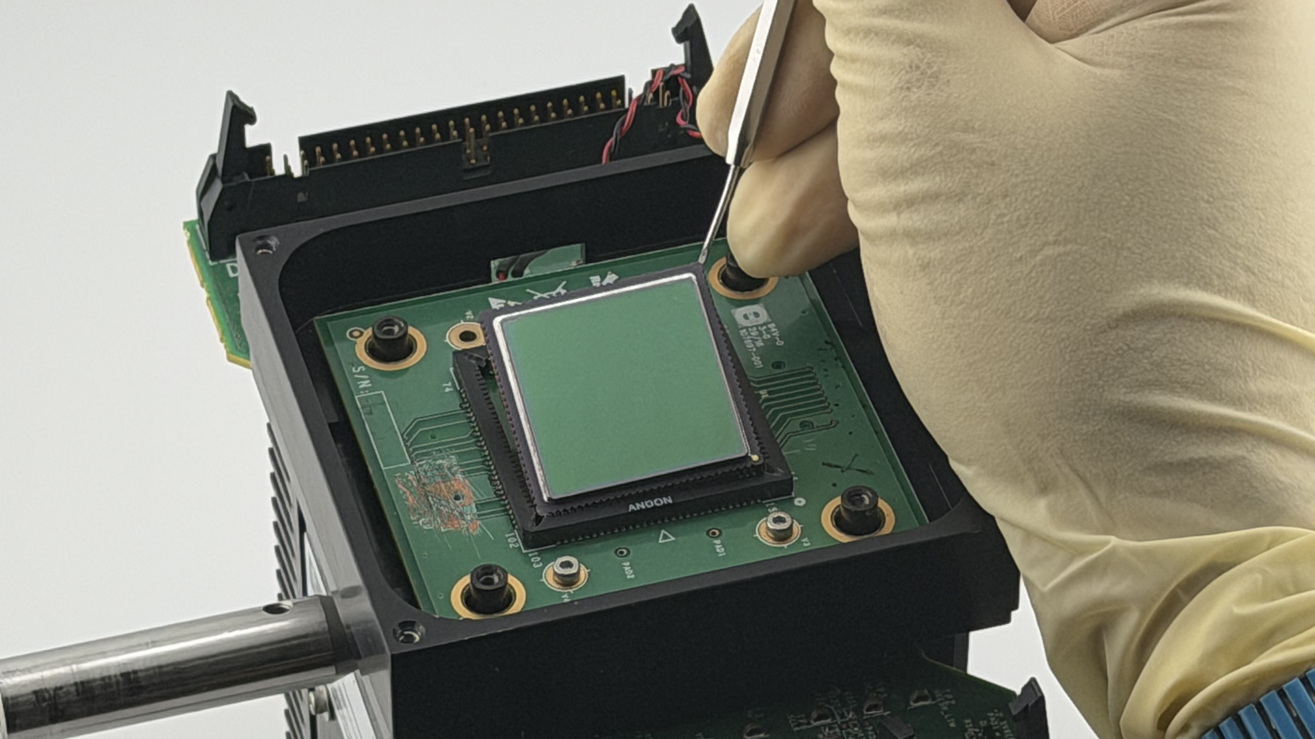
PACKAGING
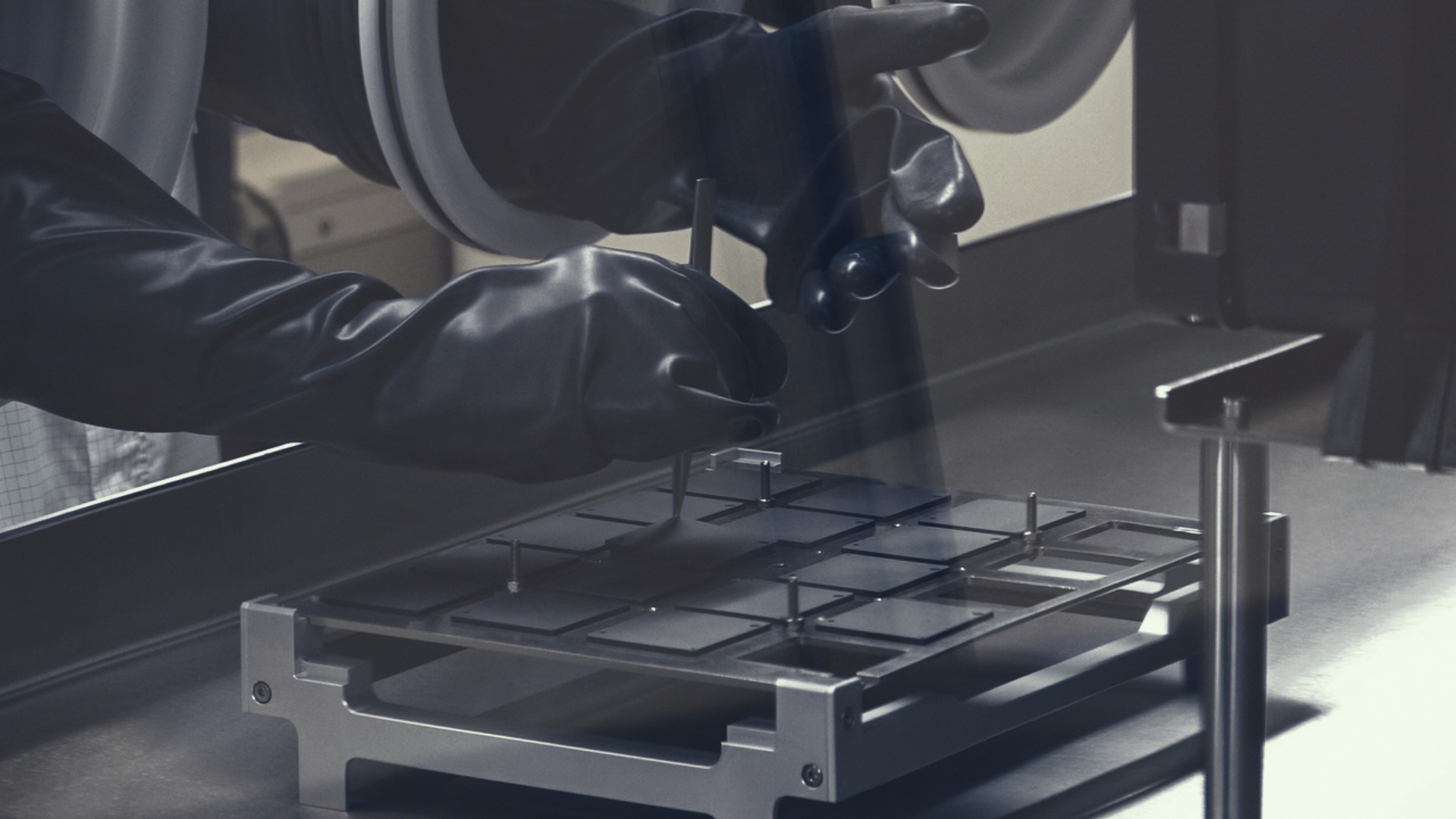
Wafer Dicing
Wafer Dicing is the process of separating individual silicon dies from a semiconductor wafer using precision cutting techniques.
Die Bonding
Die Bonding is the process of attaching a single silicon chip (die) onto a substrate or package using adhesive or epoxy methods.
Wire Bonding
Wire Bonding is the process of creating electrical connections between a silicon die and its package (or substrate) using ultra-fine wires (Gold or Aluminum).
Thermal Vacuum Sealing
Thermal sealing is the final packaging step where a protective lid or cover is hermetically sealed onto the device package using heat and high vacuum pressure.
Wafer Level Bonding
Wafer-Level Bonding is an advanced process where two or more silicon or glass wafers are permanently bonded together using thermal, or anodic techniques.
Full Integration
We provide end-to-end solutions from wafer dicing to packaging, ensuring seamless integration and high quality for your semiconductor devices.